ASPECTS OF TRANSMISSION ELECTRON MICROSCOPY IMAGE PROCESSING OF COMPOSITES CONTAINING GERMANIUM AND SILICON NANOCRYSTALS
D.A. Grachev, A.V. Ershov, D.A. Pavlov
Lobachevsky State University of Nizhni Novgorod, Russia
grachov@phys.unn.ru, ershov@phys.unn.ru, pavlov@unn.ru
Contents
Improved visualization technique and analysis of the high-resolution transmission electron microscopy images of the dielectric composite structures contained silicon and germanium crystalline nanoparticles have been performed. The modified algorithm of Wiener filtering and geometric phase processing taking into account the features of electron microscopy images both in direct and in reciprocal spaces linked by Fourier transform has been proposed and used effectively. In particular, it has been obtained counter plots of angular and spatial orientation of the nanocrystals, as well as has been measured their lateral dimensions for multilayer nanoperiodic SiOx/ZrO2 and Ge/SiO2 structures. In general, the color-layer representation of information on the electron microscopy images is a handy tool to show structure and interaction between individual structural phases of the advanced composite nanomaterials.
Keywords: Transmission electron microscopy, the geometric phase method, Wiener filter, composite material, silicon and germanium nanocrystals.
1. Introduction
Interest in obtaining nanoscale materials with unusual properties stimulated the rapid development of nanotechnology industry in the past decade. Discovery of the luminescent activity of Si [1] and Ge [2] nanoparticles in amorphous dielectric matrix — the key materials of microelectronics — was a breakthrough in researching of the composite material. For that reason the material has a broad opportunities and good prospects for nanophotonics [3]. A topic of the large number of the articles is devoted to study structure of nanoparticles. Equipment necessary to do this sort of research is a high resolution transmission electron microscope (HR-TEM) [4]. The process of image obtaining and its subsequent examination is quite a laborious and time-consuming task [5]. It is not always possible to carry out an exhaustive analysis of a microscopic image, owing to the fact that the image is partly noisy [6], there is a weak contrast of the crystalline regions, as well as the complexity of the procedures of digital processing.
To analyse HR-TEM picture in a more informative way is to use supplementary devices extending the microscope functionality. It could be electron energy loss spectroscopy Ω- and G-filters [4], [7] built in a column of the microscopy, enabling phase composition to be seen at the high resolution image [8]. Similarly, additional equipment is needed for the energy dispersive X-ray spectroscopy that allows mapping the atomic concentrations of substances in the surface layer along the line profile [9].
There is an alternative approach to analyze of
nanocrystalline inclusions which involving digital processing of the TEM
images. The method was provided by M. Hÿch et al. in the pioneering
articles [10],
[11]. It is named the geometric phase method. It is developed to extract
particular crystal phases from the microscopic picture. The key idea of the
method is applying filter mask to source image in the reciprocal space [12].
Let us remind that direct space is a space defined by the radius vectors, i.e.
this is the common coordinate space. The concept of the reciprocal space is
used in crystallography [13].
The space is determined by the basis of the wave vectors ![]() [14]–[16],
unit of which is inverse to the unit of the radius vectors
[14]–[16],
unit of which is inverse to the unit of the radius vectors ![]() ,
, ![]() . The
wave vector
. The
wave vector ![]() is
also known as spatial frequency [16].
The name is obvious due to the fact that the operation linking the direct space
to the reciprocal space is Fourier transform.
is
also known as spatial frequency [16].
The name is obvious due to the fact that the operation linking the direct space
to the reciprocal space is Fourier transform.
Typical method of the microscopic image noise reduction based on Wiener filter [17] was improved by R. Kilaas. In a paper [18] he described algorithm selecting desired information about crystalline regions on a background of the signal from amorphous matrix. The principle is found on the features of view of amorphous and crystalline region in the reciprocal space. Using the methods of statistical signal processing, the author cleaned up the image of the test structure of amorphous regions.
The statistical method has been improved by M. Seyring et al. In particular, they showed that the distribution of the noise signal from amorphous matrix along a centered ring is well described by the log-normal distribution. In a report [19] the writers describe the process of working with microscopic images of composite structures containing ensembles of nanocrystals. Implementing the geometric phase technique, the authors realized microscopic images of the same interplanar distance nanocrystals and specific crystallographic orientation.
Widespread high-resolution transmission electron microscopy and high performance of computers have led to the further development of the method of geometric phase. Therefore, there are articles on heterostructures [20], [21], where the authors analyze the crystal lattice deformation. A utilitarian innovation, which was demonstrated, for example, in P. Fraundorf’s papers [21], [22], is usage of color to highlight similar areas or to mark out certain image part, since it is a way to reduce the number of images.
We tried to apply the above-described methods for the analysis of microscopic images of structures containing nanocrystals of silicon and germanium. During the work we have faced a number of challenges, little-discussed, as we know, in papers. In particular, they are alignment contrast nanoparticles, visible with different interplanar spacings; Z-contrast influence on the shape of the noise intensity distribution; annular unevenness of noise associated with the problems of microscope calibration; features of the discreet image processing. In this article we present the results of using geometric phase technique taking into account few improvements.
2. Material and Methods
In this paper, we report on the imaging processing results of multilayer nanoperiodic SiOx/ZrO2 and Ge/SiO2 structures containing crystalline nanoparticles [23]. They were formed by vacuum evaporation from separate sources, after they had been annealed in nitrogen atmosphere. In greater detail the preparation process was described in [24].
Amorphous multilayer nanoperiodic structure of SiOx/ZrO2 was deposited by vacuum evaporating materials from two separate sources on silicon substrate at 200 ± 10 °C as in details it is described in [24]. The sample was annealed for 2 hours in a nitrogen atmosphere at a temperature 1100 °C. We used modified VU-1A machine (Smorgon Optical Machine-Tool) with a photometric layer-thickness measuring add-on.
Similarly, multilayer nanoperiodic structure Ge/SiO2 was obtained. Samples were performed by evaporation of germanium and fused silica on combined vacuum system 2G11G2-ElBeam-OQ-03 (Torr Int) equipped with oil-free pumping system and quartz thickness control system. Anneal was about 1 hour at 800 °C.
Pictures of the structures were obtained by electron transmission microscopy (JEM-2100F, JEOL). Preparation of the cross section was performed on equipment according to the Gatan’s etching procedure comprising successive steps of machining and precision ion-beam etching. Digital image processing was carried out using self-made algorithms in numerical processing systems.
3. Theory and calculations
It is reasonable to briefly describe the basic principles of the image processing. The method is based on Fourier transmission of the digitized sample picture (Fig. 1.a). We used centered [25] discrete Fourier transform (DFT) placing low frequencies in the image center and putting high frequencies on the border. In this case, the DFT image is similar to electron diffraction pattern from polycrystalline or texture [4], which looks like the series of ordered sharp bursts of intensity from the crystalline regions (reflexes, spots) against the background of low-contrast wide amorphous halo (Fig. 1.b). We deliberately do not use the FFT, since this approach introduces additional distortion; image is compressed with losses or cropped. Modern PCs do DFT in a reasonable time.
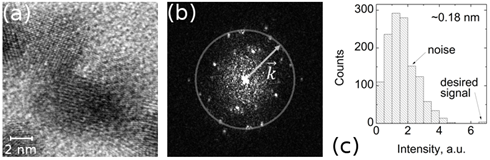
Fig. 1. Exemplary scheme of Wiener filter processing: a HR-TEM image (a), the centered DFT HR-TEM image with annular filter contour (b), statistics of the intensity along the contour (c)
Ordinary, preliminary processing of HR-TEM images involves
Wiener filter [17],
[26], which makes it possible to separate useful signal from the background
noise when we are aware of its characteristic in advance. According to
diffraction pattern properties, the noise signal from amorphous matrix (as
halo) is assumed to be degenerate in the radial direction of the spatial
frequency vector [18].
It means that intensity of the noise signal should to be a constant along a
circle contour ![]() (Fig.
1.b). In practice, we observe random deviation of intensity along a contour,
and, therefore, it has to be described with Gaussian lognormal statistics (Fig.
1.c) [19].
In consonant with the math statistics the most probable signal is noise, while
low probability deflections correspond to the desired signal. As result, the
separated data is used to provide a Wiener filter.
(Fig.
1.b). In practice, we observe random deviation of intensity along a contour,
and, therefore, it has to be described with Gaussian lognormal statistics (Fig.
1.c) [19].
In consonant with the math statistics the most probable signal is noise, while
low probability deflections correspond to the desired signal. As result, the
separated data is used to provide a Wiener filter.
It’s important to take into account the problem of quantiles choosing. If there are two types of nanocrystal differ in contrast, what can be caused by Z-contrast [4] as for the SiOx/ZrO2 system, then there are two values of the signal-to-noise ratios, and as a result it is possible to lose valuable information about lighter nanocrystals.
The approach to filtering faces two problems at least. In the first place, due to focus beam characteristics in the electron microscope [4], utilization of a contour in form of the circle is probably beside the purpose. The curve of constant intensity on DFT-image could be in the shape of an ellipse or a hyperbola (Fig. 2.a). In this connection, we have to align noise intensity in the angular direction, which makes possible the Wiener filter implementation. It is obvious that in the direct space the alignment leads to small contrast change of the original image, without significant distortions.
In the second place, it is impossible to select any curve as
a closed ring by the fact that the HR-TEM image is square. This means that it
is no way to make a circle contour for wave vector ![]() larger
than 2 (Fig. 2.b). We assume side length of the image square in the direct space
is equal to one length unit. Instead of the circumference, four arcs of the
same radius may be selected. Their total length is less than the length of a
circle in
larger
than 2 (Fig. 2.b). We assume side length of the image square in the direct space
is equal to one length unit. Instead of the circumference, four arcs of the
same radius may be selected. Their total length is less than the length of a
circle in ![]() times.
The contour length reducing leads to increase the accuracy of calculations.
However, growing of errors doesn’t affect the result of the processing, as the
useful information is rarely placed in the image corners.
times.
The contour length reducing leads to increase the accuracy of calculations.
However, growing of errors doesn’t affect the result of the processing, as the
useful information is rarely placed in the image corners.
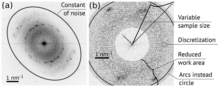
Fig. 2. Fourier transformed image (a), where curve of the constant level of noise is non-circular (elliptical), and DFT image illustrating features of the digital image processing (b)
As far as for the geometric phase method is concerned, in addition to the standard masks for individual reflexes we further modify the filtered DFT HR-TEM images in reciprocal space applying two type of masks to implement the approach shown in [19], [21]. They are annular and sector masks.
As the name of the annular mask, the first processing method is to select centered annular formed fragments (Fig. 3.a) on a DFT image. Each fragment is transferred from the reciprocal space into the direct and is painted a color according to legend. The result is a superposition of the all colored layers. From a physical viewpoint, color corresponds to the crystalline regions with the certain interplanar spacings. We used available databases of interplanar spacings [27] to pick out the desired material.
The mask for the second processing method is a couple of the
annular sectors exiting zero, area where ![]() 0
(Fig. 3.b). Superposition of this type mask and ring makes it possible to show
angular orientation of crystal fragments with the specified interplanar
spacings (Fig. 3.c). The presence of the annular filter is necessary, since one
and the same nanocrystal is able to be seen from different angles for different
interplanar spacings [4],
[28], [29], furthermore, that helps cutting off excess noise.
0
(Fig. 3.b). Superposition of this type mask and ring makes it possible to show
angular orientation of crystal fragments with the specified interplanar
spacings (Fig. 3.c). The presence of the annular filter is necessary, since one
and the same nanocrystal is able to be seen from different angles for different
interplanar spacings [4],
[28], [29], furthermore, that helps cutting off excess noise.
Finally, in order to reduce noise signal and improve the image processing methods, we have used a set of standard masks for the geometric phase technique. It is a set of circles (Fig. 3.c), where center of each hole coincides with the spot position, and their radii are about to the ring filter width. Thus, each mask is inhibiting signal passing except for the specific spots.

Fig. 3. Typical annular (a), sector (b), and geometric-phase (c) masks
It is necessary to discuss the distortions induced by the
masking process. In mathematical terms the masking operation is a product of
DFT-HR-TEM image by the mask image. Multiplication of functions in reciprocal
space is equivalent to their convolution in direct space [25].
In our case it means that applying the mask leads to image blurring [30].
At the same time, the smaller the width of the filter ring, the stronger is the
blur. However, due to the fact that the blur radius is of the order of about
interplanar spacings, the reconstructed image seems to be reliable. The above
can be proved if one notes that in the radial direction the ring mask is a
rectangle function of the type ![]() [16].
In direct space it looks like
[16].
In direct space it looks like ![]() .
.
Further it is desirable to provide a survey of the operation of annular masking and forming a color image (Fig. 4). As mentioned earlier, the algorithm consists of retrieving the filtered images (Fig. 4.c) from reciprocal space, coloring them in a distinctive manner in direct space (Fig. 4.d), and merging them together. To get the contrast image, it requires extra processing step. In the paper [19] this question was formulated but had remained unsettled. The problem is that a part of the nanocrystals look low contrast, due to the different crystal abilities to diffraction electron in different directions. To emphasize the largest number of nanocrystals and make them stand on background noise, average intensity of any retrieved images is normalized separately. We empirically found out that the optimal ratio of the average value to the maximum intensity is about 0.3.
Considering the image margin process it is advisable to focus on color mixing. The retrieved images are given color in such way that dark areas become transparent, and bright areas have a special color. Color overlay occurs according to the law of their mixing [31]. With the purpose of avoiding ambiguity in the interpretation of colors, we suggest using colors unevenly placed on the scale shades as a legend. Alternatively, when there are a number of legend items, the results can be interpreted in terms of brightness, since it should be greater when nanocrystals overlapped. The background color is actually black, but, for clarity it was partly shown the intensity-inverted images.
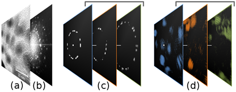
Fig. 4. The annular filter processing: HR-TEM image (a), the DFT image (b), a set of the filtered DFT images (c), the retrieved and pained corresponding (d) images
In general, this image processing can be effectively used for crystalline regions phase indicating, the result comparable with energy-microscope work. The difference is that the method discussed in the paper is not sensitive to amorphous clusters, and consequently countable number of clusters in the image reduces.
4. Results and discussion
For the SiOx/ZrO2 structure a preliminary analysis of the spots allowed assuming that there are at least two types of nanocrystals. They are composed of pure silicon and a silicon-zirconium compound. Based on this suggestion we formed two masks consisting of a series of filtering rings for these materials respectively. Filter parameters are presented in Table 1. There were consistently applied 9 different masks in the form of ring. A univocal choice inner and outer radii of annular mask is complicated by the proximity of the spots, corresponding to different interplanar spacings. For rings correlated with pure silicon (structural form of Fd3m) reference data are given [32], [27]. To find out a particular formula of silicon-zirconium compound is necessary to do more researches further.
A comprehensive figure 5 shows the result of image processing for SiOx/ZrO2 structure. The first figure, on the top left corner, is an initial HR-TEM image (Fig. 5.a). Separately, images of pure silicon and of silicon-zirconium compound are presented in figures 5.b and 5.c respectively. Here a color indicates crystalline regions corresponding to one value of the interplanar spacings. Totally there are seven colors, as amount of the interplanar spacings. For other values filtered images are not informative. As a whole phases are shown in a complex dichromatic figure (Fig. 5.d). Green color symbolizes the phase of pure silicon, and blue does the silicon-zirconium compound. Now it seems to be obvious that we see one big silicon nanocrystal and a lot of ordered small nanocrystals of silicon-zirconium compound.
Table 1. Annular filter parameters for the SiOx/ZrO2 structure
|
# |
Radii of inner and outer filter boundaries, nm-1 |
Average value of interplanar spacings, nm |
Reference Si interplanar spacings, nm |
|
1 |
3.03 – 3.25 |
0.318 ± 0.023 |
0.313 |
|
2 |
3.25 – 3.57 |
0.293 ± 0.027 |
|
|
3 |
3.57 – 3.79 |
0.271 ± 0.016 |
0.272 |
|
4 |
3.79 – 4.12 |
0.253 ± 0.021 |
|
|
5 |
4.64 – 4.88 |
0.210 ± 0.010 |
|
|
6 |
5.08 – 5.32 |
0.192 ± 0.008 |
0.192 |
|
7 |
5.32 – 5.95 |
0.177 ± 0.020 |
|
|
8 |
5.95 – 6.24 |
0.164 ± 0.008 |
0.163 |
|
9 |
6.24 – 6.62 |
0.156 ± 0.009 |
|
The sector principle of filtering was realized with the object of obtaining a map of the spatial orientation of crystal fragments, as mentioned previously. Separately for each value of the interplanar spacings the angular orientation map was calculated and was show in figures 5.e-5.m. In this case, angles are referred to by colors (see the legend at the bottom right). It is observed that there are some isolated areas with a preferred orientation. The reasons for that behavior of systems require additional research.
Quite apart from the SiOx/ZrO2 structure, we investigated a similar sample containing nanocrystals of germanium, since there is an intensive study of such systems [33] now days. Particularly, we have processed the system multilayer nanoperiodic Ge/SiO2 [34].
At the figure there are several peculiarities of processing. The first noticeable thing is not all dark round areas of the original image defined as the crystal. This is due to operation of the electronic transmission microscope. If one evaluates amount of particles, the total number will be underestimated. Also, there is allegedly visible imposition of different compositing nanocrystals. In earnest, a part of them don't overlap and are arranged one above the other. Other part is an artifact of processing. When spot size is comparable to thicknesses of filter ring, then it takes account of neighboring extrinsic spots. This type artifact is difficult for analysis; in this case the filtering method couldn't to exhaust the topic subject.
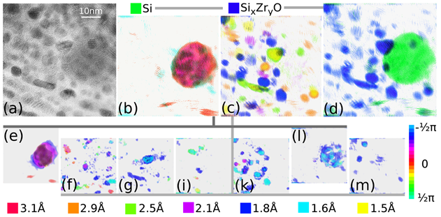
Fig. 5. HR-TEM Images of SiOx/ZrO2 structure: before treatment (a), processed for pure silicon only (b), processed solely for silicon-zirconium compound (c), combined image (d), the angular orientation maps of nanocrystals for identifired interplanar spacings (e-m)
An initial image fragment of the image is shown in Fig. 6.a,
while Fig. 6.b does the result of the color processing. Three values of the
interplanar spacings are observed there. They are 0.33 nm (Fig. 6.c), 0.20 nm
(Fig. 6.d), and 0.17 nm (Fig. 6.e), corresponding to Ge structure Fd3m. It
means that just vertically arranged packed layers of Ge nanocrystals in
amorphous matrix are observed. As far as color legend for figures 6.c, 6.d and
6.e, color symbolize angle subtended a particular nanocrystal. The angle varies
from ![]() to
to ![]() ,
which is a half of the circle. Explanation is that the absolute value of signal
in inverse space is equal to itself in diametrically opposite direction. Note
that some nanocrystals look “striped” and filled with low spatial frequencies.
Thus manifested moiré pattern [4]
caused by overlapping supervision of nanocrystals.
,
which is a half of the circle. Explanation is that the absolute value of signal
in inverse space is equal to itself in diametrically opposite direction. Note
that some nanocrystals look “striped” and filled with low spatial frequencies.
Thus manifested moiré pattern [4]
caused by overlapping supervision of nanocrystals.
From the figure showing angular orientation (Fig. 6.d-e) it follows that there are groups of germanium nanocrystals possessed of the same orientation. The nanocrystals closely arranged in layers interact with each other, and inevitably form clusters. The clusters are in view just for one value of the interplanar spacings. One and the same nanocrystal may be visible as an object with multiple interplanar spacings, but in this case the relation between the angles specific and determined by the structure of the crystal lattice.
Comparing the results of annular (Fig. 6.b) and sector (Fig. 6.d-e) image filtration processing, one can see that the painted over area looks larger in the second case. The artifact of spreading color area into the amorphous matrix was presumably resulted in high discretization of the sector mask. Each restore operation begets image blurring. The more transactions, the less clear the picture becomes. It is necessary keep a balance between informativeness and accuracy.
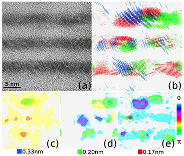
Fig. 6. HR-TEM Images of Ge/SiO2 structure: before treatment (a), processed with anular mask filter showing equal interplanar distances earies (b), the angular orientation map of nanocrystals for interplanar spacings 0.33 nm (c), map for interplanar spacings 0.20 nm (d), map for interplanar spacings 0.17 nm (e)
5. Conclusion
In the paper we present the results of using the image processing technique for electron microscopy pictures containing crystalline nanoinclusions. Using the improved masking principle based on the selection of certain spatial frequencies in reciprocal space, known as geometric phase method, few crystalline phases in a complex composite material SiOx/ZrO2 were highlighted. As far as the Ge/SiO2 structure, analysis of crystallographic orientation nanoinclusions was demonstrated, which showed a weak angular correlation between adjacent nanocrystals of indentical composition. On the whole, local phase analysis is an informative tool to investigate multi component nanostructured materials based on silicon and germanium.
The algorithm under consideration had basically an academic focus, since standard approaches were not quite clear and suitable to process images of the solid nanocomposites. In view of the fact that all the key features of the method have been described in the text, we see no obstacles for its shared usage or mutual further development.
Acknowledgements
The work was partially supported by the Russian Foundation for Basic Research (RFBR) project 14-02-00119.
References
[1] Cahay M., Bandyopadhyay S. Device Applications of Silicon Nanocrystals and Nanostructures. Springer Science & Business Media, 2009.
[2] Gerung H. Nanocrystals – Synthesis. Characterization and Applications. InTech, 2012.
[3] Mascher P. Nanocrystal Embedded Dielectrics for Electronic and Photonic Devices. The Electrochemical Society, 2009.
[4] David C. B. C., Willams B. Transmission Electron Microscopy: A Textbook for Materials Science. New York: Springer, 2009.
[5] Ayache J., Beaunier L., Boumendil J. J., Ehret G., Laub D. D. Sample Preparation Handbook for Transmission Electron Microscopy. Springer Science & Business Media, 2010.
[6] Krumeich F., Müller E., Wepf R.A. Phase-contrast imaging in aberration-corrected scanning transmission electron microscopy. Micron, vol. 49, pp. 1–14, Jun. 2013.
[7] Brundle M., Evans C.A., Wilson S. Encyclopedia of Materials Characterization: Surfaces, Interfaces, Thin Films. Gulf Professional Publishing, 1992.
[8] Prestat E. Quantitative TEM and STEM study of Pt-Nanoparticles Coarsening and Ge(Mn)-based Ferromagnetic Semiconductors. Theses, Université de Grenoble, Karlsruher Institut für Technologie, 2013.
[9] Bell D., Garratt-Reed A. Energy Dispersive X-ray Analysis in the Electron Microscope. Garland Science, 2003.
[10] Hÿch M. J., Potez L. Geometric phase analysis of high-resolution electron microscopy images of antiphase domains: Example Cu 3 Au. Philos. Mag. A, vol. 76, no. 6, pp. 1119–1138, Dec. 1997.
[11] Hytch M.J. Analysis of Variations in Structure from High Resolution Electron Microscope Images by Combining Real Space and Fourier Space Information. Microsc. Microanal. Microstruct., vol. 8, no. 1, pp. 41–57, 1997.
[12] Rodenburg J. M. Reciprocal space and the reciprocal lattice. 2004. [Online]. Available: http://www.rodenburg.org/theory/Reciprocalspace20.html. [Accessed: 20-Sep-2016].
[13] Zou X., Hovmöller S., Oleynikov P. Electron crystallography: electron microscopy and electron diffraction. Oxford University Press, 2011.
[14] Cohen M. L., Louie S. G. Fundamentals of condensed matter physics. Cambridge University Press, 2016.
[15] Zhang K., Li D. Electromagnetic theory for microwaves and optoelectronics. Springer, 2008.
[16] Tang K. T. Mathematical methods for engineers and scientists, vol. 3. Springer, 2007.
[17] Marks L.D. Wiener-filter enhancement of noisy HREM images. Ultramicroscopy, vol. 62, no. 1–2, pp. 43–52, 1996.
[18] Kilaas R. Optimal and near-optimal filters in high-resolution electron microscopy. Microsc., vol. 190, no. 1–2, pp. 45–51, 1998.
[19] Seyring M., Song X., Chuvilin A., Kaiser U., Rettenmayr M. Characterization of grain structure in nanocrystalline gadolinium by high-resolution transmission electron microscopy. J. Mater. Res., vol. 24, no. 2, pp. 342–346, 2009.
[20] Gutakovskii A. K., Chuvilin A., Song S.A. Application of high-resolution electron microscopy for visualization and quantitative analysis of strain fields in heterostructures. Bull. Russ. Acad. Sci. Phys., vol. 71, no. 10, pp. 1426–1432, Oct. 2007.
[21] Fraundorf P., Fei L. Digital Darkfield Decompositions. Microsc. Microanal., vol. 10, no. Supplement S02, pp. 300–301, 2004.
[22] Fraundorf P. Digital Darkfield Analysis of Lattice Fringe Images with ImageJ. Microsc. Microanal., vol. 20, no. Supplement S3, pp. 824–825, 2014.
[23] Barbagiovanni E.G., Lockwood D.J., Simpson P.J., Goncharova L.V. Quantum confinement in Si and Ge nanostructures: Theory and experiment. Appl. Phys. Rev., vol. 1, no. 1, p. 11302, Mar. 2014.
[24] Ershov A.V., Pavlov D.A., Grachev D.A., Bobrov A.I., Karabanova I.A., Chugrov I.A., Tetelbaum D.I. Annealing-induced evolution of the structural and morphological properties of a multilayer nanoperiodic SiOx/ZrO2 system containing Si nanoclusters Semiconductors, vol. 48, no. 1, pp. 42–45, Jan. 2014.
[25] Broughton S.A., Bryan K. Discrete Fourier Analysis And Wavelets; Applications To Signal And Image Processing. Hoboken, N.J: Wiley, 2009.
[26] Lin F., Jin C. An improved Wiener deconvolution filter for high-resolution electron microscopy images. Micron, vol. 50, pp. 1–6, 2013.
[27] Mirkin L.I., Umanskii J.S., Bradley J.E.S. Handbook of X-Ray Analysis of Polycrystalline Materials. New York: Consultants Bureau, 1964.
[28] Pavesi L., Turan R. Silicon Nanocrystals: Fundamentals, Synthesis and Applications. John Wiley & Sons, 2010.
[29] Goodhew P.J., Humphreys J., Beanland R. Electron Microscopy and Analysis, Third Edition, vol. 30. CRC Press, 2000.
[30] Downing K.H., Glaeser R.M. Restoration of weak phase-contrast images recorded with a high degree of defocus: The ‘twin image’ problem associated with CTF correction. Ultramicroscopy, vol. 108, no. 9, pp. 921–928, Aug. 2008.
[31] Burger W., Burge M. Principles of Digital Image Processing. London: Springer London, 2009.
[32] Gorelik S.S., Rastorguev L.N., Skakov I.A. Rentgenograficheskiĭ i ėlektronnoopticheskiĭ analiz. Prilozheniia, Metallurgi. Moskva, 1970.
[33] Lepadatu A.M., Stoica T., Stavarache I., Teodorescu V.S., Buca D., Ciurea M.L. Dense Ge nanocrystal layers embedded in oxide obtained by controlling the diffusion-crystallization process. J. Nanoparticle Res., vol. 15, no. 10, pp. 1–12, Sep. 2013.
[34] Grachev D.A., V A. Ershov, Surovegina E.A., V A. Nezhdanov, V A. Pirogov, Pavlov D.A. Optical and structural properties of annealed multilayered nanoperiodic structures Ge/SiO2 containing germanium nanocrystals. Vestn. Lobachevsky State Univ. Nizhni Novgorod, vol. 1, no. 2, pp. 59–63, 2014.
АСПЕКТЫ ОБРАБОТКИ ИЗОБРАЖЕНИЙ ПРОСВЕЧИВАЮЩЕЙ ЭЛЕКТРОННОЙ МИКРОСКОПИИ КОМПОЗИТНЫХ СТРУКТУР, СОДЕРЖАЩИХ НАНОКРИСТАЛЛЫ ГЕРМАНИЯ И КРЕМНИЯ
Д.А. Грачев, А.В. Ершов, Д.А. Павлов
Нижегородский государственный университет им. Н. И. Лобачевского, Россия
grachov@phys.unn.ru, ershov@phys.unn.ru, pavlov@unn.ru
Представлены результаты усовершенствованного подхода к визуализации и анализу снимков просвечивающей электронной микроскопии высокого разрешения диэлектрических композитных материалов, содержащих кристаллические нановключения кремния и германия. Предложен и эффектно применен модифицированный алгоритм геометрической фазы и Винеровской фильтрации, учитывающий особенности изображений электронной микроскопии нанокомпозитов как в прямом, так и в обратном пространствах, связанных операцией Фурье преобразования. В частности, для многослойных нанопериодических структур SiOx/ZrO2 и Ge/SiO2 были получены карты углового и пространственного распределения нанокристаллических фаз, а также данные их латеральных размеров. В целом описанная многослойная цветовая интерпретация информации на снимках электронной микроскопии позволяет наглядно отразить строение и взаимодействие отдельных фазовых включений современных композитных наноматериалов.
Ключевые слова: Просвечивающая электронная микроскопия, метод геометрической фазы, Винеровская фильтрация, композитный материал, нанокристаллы кремния и германия.